Precision Manufacturing: The Core Support of Semiconductor Equipment
The advancement of semiconductor technology is deeply rooted in the extreme precision and reliable performance of the manufacturing process. The realization of nanoscale circuits demands that the key components of supporting equipment meet unprecedented standards at the microscopic level. Precision CNC machining, semiconductor-grade brazing processes, and a profound understanding of the semiconductor manufacturing environment form the cornerstone for meeting these stringent requirements.
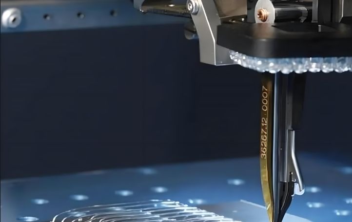
CNC: The Physical Basis for Semiconductor-Level Precision
The requirements of semiconductor equipment for geometric tolerance and surface integrity define the limits of precision manufacturing. Achieving sub-micron features relies on high-precision CNC technology. Multi-axis machine tools, integrated with real-time feedback mechanisms to correct machining paths, can converge critical dimensions to within ±2 microns, even when dealing with materials like alumina ceramics or Kovar alloy. The core challenges lie in how to ensure nanoscale dimensional stability of vacuum sealing surfaces under 300°C thermal cycling and how to eliminate particulate contamination induced by machining residues. It is this ability to control microphysical properties that defines the reliability boundaries for components such as electrostatic chucks and gas showerheads.
Brazing Process: Reliable Connections in Extreme Environments
The semiconductor manufacturing environment poses comprehensive challenges to components: vacuum seal failure, thermal stress cracking, and minor reactions between materials can all lead to fatal defects. Against this backdrop, the value of brazing processes is highlighted. Compared to mechanical connections or adhesives, the metallurgical bonding interface created by brazing possesses intrinsic cleanliness, excellent gas tightness, and inherent strength. Choosing to braze vacuum chamber flanges, cooling lines, or sensor packages is essentially seeking long-term compatibility between the joints and the service environment, such as continuous ultra-high vacuum conditions, periodic plasma exposure, and instantaneous temperature changes of hundreds of degrees Celsius. In practice, the oxide-free connection of large metal components often relies on brazing in a rotary furnace with precise hydrogen control; while achieving reliable bonding between copper alloy pipes and stainless steel chamber walls near precision sensors requires engineers to manually control millimeter-scale local heat input with microtorches. When conductivity or thermal conductivity becomes the primary consideration, the selection of gold-based or nickel-based brazing filler metals becomes crucial — subtle differences in their properties can cause key system parameters to fluctuate by more than 15%.
Semiconductor Manufacturing Environment: The Underlying Logic of Process Design
Serving semiconductor equipment demands that the manufacturing process goes beyond mere machining capabilities. Components must reliably operate under the stringent cleanliness stability and long-life requirements of a wafer fabrication facility. This means that material selection must consider extremely low outgassing rates and corrosion resistance; the machining environment must control particulate levels; structural design must optimize thermal stress distribution; and cleaning and passivation processes must ensure the intrinsic cleanliness of surfaces. Understanding the operating principles of semiconductor equipment directly affects the design of structural stiffness for wafer transfer mechanisms, matching the thermal expansion coefficients of internal components in reaction chambers, or implementing anti-interference shielding solutions for measurement probes. For example, optimizing the CNC machining allowance distribution and brazing sequence of the ceramic substrate of an electrostatic chuck significantly reduced its deformation during high- and low-temperature cycling.
Technological Convergence: Systematic Solutions for Complex Challenges
The manufacturing of cutting-edge semiconductor equipment components is often a deeply collaborative process between precision CNC forming and reliable brazing connections. Typical examples include aluminum alloy vacuum chambers with internally brazed copper cooling lines, which require CNC machining to ensure sealing surface accuracy while brazing processes guarantee the vacuum tightness of the cooling circuit; or ceramic-metal composite electrostatic chuck electrode structures, which rely on CNC to achieve precise ceramic substrate morphology and micro-holes, and on high-temperature brazing to achieve a strong bond with the metal layer. The successful delivery of such projects depends on cross-process teams' shared understanding and collaboration on semiconductor application scenarios. For instance, a vacuum mechanical arm joint component, with its titanium alloy main body CNC machined and integrated with brazed sensors and ceramic insulators, requires simultaneous solutions for lightweight signal shielding and vacuum compatibility.
Evolution of Manufacturing Capabilities for Future Nodes
As semiconductor technology continues to evolve towards smaller feature sizes, higher power densities, and more complex structures, it poses ongoing challenges to its manufacturing foundation. This is reflected in the need to develop CNC process parameters and new types of brazing filler metals for new material applications; the push for more precise CNC micro-machining and localized brazing technologies by three-dimensional integrated structures; and the testing of long-term stability of heterogeneous material brazing interfaces by extreme thermal management requirements. The continuous improvement of precision CNC machining and advanced brazing processes is the underlying guarantee for the performance breakthroughs of next-generation semiconductor equipment. For example, the manufacturing of high-power device heat sinks is driving the maturity of active metal brazing processes for aluminum nitride and copper combinations, while the machining of micro-reactor chambers relies on the CNC capabilities of ultra-high-speed micro-milling technology. The iteration of technological capabilities always serves the ever-upgrading performance requirements of semiconductor equipment.